PhD Thesis defense: "Thermal, stress, and traps effects in AlGaN/GaN HEMTs" by Mr. Ashu Wang
On Friday, October 3, 2014, at 12:00, at the "Salón de Grados" - Building A of the ETSI Telecomunicación, will take place the PhD thesis defense of Mr. Ashu Wang, which is entitled: "Thermal, stress, and traps effects in AlGaN/GaN HEMTs" and has been realized under the supervision of Prof. Fernando Calle Gómez and Dr. Marko Jak Tadjer.
Abstract:
GaN and AlN are group III-V piezoelectric semiconductor materials. The AlGaN/GaN heterojunction presents large piezoelectric and spontaneous polarization charge at the interface, leading to high 2DEG density close to the interface. A high power output would be obtained due to the high 2DEG density and mobility, which leads to elevated lattice temperature. The gate and drain biases induce converse piezoelectric stress that can influence the piezoelectric polarization charge and further influence the 2DEG density and output characteristics. Therefore, the device physics is relevant to all the electrical, thermal, and mechanical aspects. In this dissertation, by using the commercial finite-element-method (FEM) software COMSOL, we achieved the GaN HEMTs simulation with electro-thermal, electro-mechanical, and electro-thermo-mechanical full coupling. The coupling parts include the drift-diffusion model for the electron transport, the thermal conduction, and the piezoelectric effect. By simulations and some experimental characterizations, we have studied the device thermal, stress, and traps effects described in the following.
The device geometry impact on the self-heating was studied by electro-thermal simulations and electrical characterizations. Among the obtained interesting results, we found that, for same power output, the distance between the gate and drain contact can influence distribution of the heat generation in the channel and thus influence the channel temperature.
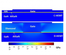
Diamond possesses high thermal conductivity. Integrated diamond with the device can spread the generated heat and thus potentially reduce the device self-heating effect. Electro-thermal simulations on this topic were performed. For the diamond integration on top of the device (top-side heat spreading), the determinant factors for the heat spreading ability are the diamond thickness, its thermal conductivity, and its distance to the heat source. The top-side heat spreading can also reduce the impact of thermal boundary resistance between the buffer and the substrate on the device thermal behavior. The very low electrical conductivity of diamond allows that it can directly contact the gate metal (which is very close to the heat source), being quite convenient to reduce the self-heating for the device under pulsed bias. Also, the diamond coated in vias etched in the substrate as heat spreading path (back-side heat spreading) was simulated. A competing mechanism influences the heat spreading ability, i.e., the etched vias would increase the device temperature due to the reduced heat sink while the coated diamond would decrease the device temperature due to its higher thermal conductivity. Therefore, relative thick coated diamond is needed in order to reduce the self-heating effect.
The simulated local stress at the gate edge of the drain side for the device with standard and field plate gate structure were compared, which would be relevant to the device mechanical failure. Other stress simulations focused on the intrinsic stress in the diamond capping layer impact on the device electrical behaviors. The simulated stress and electrical output characteristics were compared to experimental data obtained by micro-Raman spectroscopy and electrical characterization, respectively. Results showed that the intrinsic stress in the capping layer caused the non-uniform distribution of 2DEG in the channel and the access region. Besides the enhancement of the device power output, intrinsic stress in the capping layer can potentially improve the device reliability by modulating the local stress at the gate edge of the drain side.
Finally, the surface, buffer, and barrier traps effects were simulated in this work. Pulsed measurements showed that long gates and distances between gate and drain contact can increase the gate lag ratio (decrease the current collapse). This was explained by simulations on the surface traps effect. The simulations on buffer traps effects focused on illustrating the dynamic trapping/detrapping in the buffer and the self-heating impact on the device transient drain current. A model was presented to describe the trapping and detrapping in the barrier. The trapping was the electron direct tunneling from the gate metal while the detrapping was the electron emission into the conduction band described by phonon-assisted tunneling. The reverse gate current was simulated based on this model, whose mechanism can be attributed to the temperature and electric field dependent electron emission in the barrier. Furthermore, the mechanism of the device bias via the self-heating and electric field impact on the electron emission and the transient drain current were also illustrated.
